DC/DC converters that make yield voltages by intermittently pumping charge onto a capacitor as opposed to exchanging current through an inductor. Charge-pump-based voltage direction is an essential other option to the more typical inductor-based approach; charge-pump circuits
- are less complex and more affordable;
- require less PCB territory;
- offer brilliant productivity at low load current; and
- try not to produce as much transmitted EMI.
The essential constraint with charge-pump controllers is yield current; inductor-based switchers are a superior decision when you require more than around 50– 100 Mama. Be that as it may, 50 Mama is a lot of current for some low-control electronic gadgets or subcircuits, and I can't help suspecting that the attention on inductor-based DC/DC transformation has made numerous fashioners disregard a conceivably predominant option.
USB In, ±5 V Out
I made a reference plan for a power supply hinder that takes a 5 V input and produces +5 V and – 5 V yield rails. It would not be hard to alter this circuit for various voltages, however I believe that the 5 V to ±5 V arrangement could be valuable in numerous applications, since 5 V is the thing that you get from USB control (which is advantageously accessible all over the place) and in light of the fact that ±5 V is appropriate for an extensive variety of simple circuits. Additionally, 5 V is a decent place to begin on the off chance that you need to produce 3.3 V utilizing a LDO, so perhaps you could utilize the positive 5 V rail for simple hardware and furthermore direct it down to 3.3 V for advanced hardware.
A note with respect to the double supplies: There is presumably that numerous simple circuits can be executed in a solitary supply condition, and this approach can be worthwhile. In any case, my genuine belief is that simple circuits are more clear and more instinctive when bipolar supplies are utilized. I am the last individual who might need to confuse an outline with pointless power-supply hardware, however the charge-pump circuit introduced in this article is so basic and minimized that it makes bipolar supplies a plausible alternative for some simple and blended flag gadgets.
The LTC3265
The focal part in this circuit is the LTC3265 from Direct Tech/Simple Gadgets.
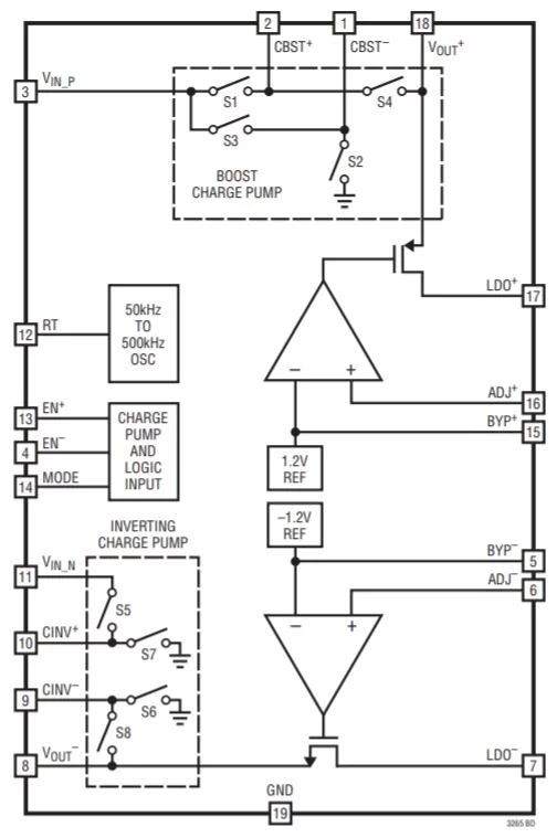
Diagram taken from the LTC3265 datasheet.
It's an exceedingly coordinated part that fuses a voltage-multiplying charge pump, a voltage-altering charge pump, and two straight controllers. Here's the manner by which I approach producing symmetric, low-commotion rails:
- The info voltage encourages the multiplying charge pump.
- The yield of the multiplying charge pump encourages the altering charge pump.
- The yields from the multiplying and altering run after pumps are managed to the coveted voltage utilizing the LDOs.
.

There are different approaches to actualize the LTC3265. You could transform the info voltage and after that utilization the information voltage and the upset voltage as your bipolar rails, or rearrange and twofold the information voltage and after that utilization a LDO to control just the multiplied voltage, or utilize the multiplied voltage to nourish the inverter and associate the multiplied and altered yields straightforwardly to the heap (i.e., without utilizing the LDOs).
In any case, the setup that I use in the reference configuration is ideal much of the time:
- It's profoundly adaptable: In the wake of creating ±10 V from the doubler and inverter, you can pick distinctive last yield voltages basically by changing two resistors. The LDO voltages are set as takes after:
VLDO+ =1.2V×(R3R1+1) VLDO−=−1.2V×(R4R2+1)
- Utilizing the LDOs to deliver the yield rails stifles the commotion produced by the exchanging activity of the charge pumps.
- The LDOs likewise guarantee that the yield rails will have an enduring voltage, regardless of whether there are huge varieties in the info voltage.
I should specify one detail before we talk about different parts of the schematic: I've alluded to the charge pumps as "multiplying" and "rearranging," yet the full story is more confounded. The LTC3265 can work either in burst mode or in open-circle mode. In open-circle mode, the lift charge pump builds its information voltage by a factor of two and the modifying charge pump increases its information voltage by negative one. In burst mode, in any case, the components are marginally littler: VBOOST = 0.94 × 2 × VIN_BOOST, and VINV = – 0.94 × VIN_INV. This doesn't generally influence my circuit, however, on the grounds that the little contrast won't change the voltage created by the LDO.
Schematic Subtle elements
Here is the whole schematic for my inductorless bipolar power supply:

- Power enters through a regular USB Smaller scale B connector.
- I incorporated an expansive capacitor on the info since I generally like a lot of capacitance when the board's information voltage is getting through a link or potentially from an obscure source. Be that as it may, the 47 µF capacitor altogether builds board size and cost (particularly cost), so in the event that you have budgetary or space imperatives, consider disposing of C1.
- The measure of obstruction between the RT stick and ground decides the LTC3265's oscillator recurrence. I utilized a potentiometer so I could try different things with various frequencies.

- J3 and J4 are female headers that I can use to embed antiquated through-opening resistors. This enables me to assess the execution of the circuit under various stacking conditions.
- C8 and C9 are not fundamental, but rather you should incorporate them since they decrease the measure of commotion in the LDO's yield voltage.
Conclusion
As should be obvious from the schematic, a section like the LTC3265 enables you to create low-clamor bipolar power supplies without broad plan exertion and without a considerable rundown of segments. (I'm accepting that the LDOs will evacuate the majority of the exchanging commotion; I'll know without a doubt after I have an opportunity to test the board.) However absolutely not a high-current power supply, the circuit can give up to 100 Mama (50 Mama from each LDO), which is all that anyone could need for some applications.
Utilizing the LDOs to deliver the yield rails stifles the commotion produced by the exchanging activity of the charge pumps.
J3 and J4 are female headers that I can use to embed antiquated through-opening resistors. This enables me to assess the execution of the circuit under various stacking conditions.
C8 and C9 are not fundamental, but rather you should incorporate them since they decrease the measure of commotion in the LDO's yield voltage.
Conclusion
As should be obvious from the schematic, a section like the LTC3265 enables you to create low-clamor bipolar power supplies without broad plan exertion and without a considerable rundown of segments. (I'm accepting that the LDOs will evacuate the majority of the exchanging commotion; I'll know without a doubt after I have an opportunity to test the board.) However absolutely not a high-current power supply, the circuit can give up to 100 Mama (50 Mama from each LDO), which is all that anyone could need for some applicatiThe LDOs likewise guarantee that the yield rails will have an enduring voltage, regardless of whether there are huge varieties in the info voltage.
I should specify one detail before we talk about different parts of the schematic: I've alluded to the charge pumps as "multiplying" and "rearranging," yet the full story is more confounded. The LTC3265 can work either in burst mode or in open-circle mode. In open-circle mode, the lift charge pump builds its information voltage by a factor of two and the modifying charge pump increases its information voltage by negative one. In burst mode, in any case, the components are marginally littler: VBOOST = 0.94 × 2 × VIN_BOOST, and VINV = – 0.94 × VIN_INV. This doesn't generally influence my circuit, however, on the grounds that the little contrast won't change the voltage created by the LDO.
Schematic Subtle elements
Here is the whole schematic for my inductorless bipolar power supply:


0 comments:
Post a Comment